Inkjet & Digital Printing
Dainippon Screen Launches Fine Line Direct Imaging System for PCB
Monday 03. June 2013 - Expanded Ledia Series Lineup Targets New Market Needs
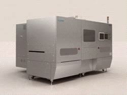
Dainippon Screen Mfg. Co., Ltd. has developed the Ledia 5F, a direct imaging system supporting pattern formation for the package PCB used in increasingly miniaturized and high-precision smartphones and tablet PCs. Sales of the Ledia 5F are scheduled to begin in June.
In recent years, in conjunction with the rapid penetration of smartphones and tablet PCs, demand has increased for the package PCB required for mounting LSI such as IC chips on to main PCB. Conventionally, the pattern formation of solder resist, a protective insulation layer coated on to the surface of PCB, used an exposure method employing photo masks. However, with the increasing miniaturization and density of PCB, a more precise pattern formation method was required. This made the achievement of both more accurate imaging and higher throughput a matter of great urgency for all PCB manufacturers.
Based on these industry trends and background, Screen has developed the Ledia 5F high-precision direct imaging system. This model inherits the industry leading* productivity and ability to handle various types of photosensitive materials featured by the Ledia 5S, released in January 2012. It also offers great flexibility, supporting line widths of 15 ?m for circuit to solder resist pattern formation. It possesses particular strengths in the formation of the high-precision solder resist patterns required for package PCB. In addition, the adoption of the Ledia series’ highly regarded high-intensity UV-LED as the light source for the Ledia 5F’s exposure head has enabled a longer operational life and lower running costs.
With this addition to the Ledia series lineup, Screen intends to acquire the top share in the direct imaging system field. It also hopes to answer the needs of various customers in the PCB industry and contribute to the expansion of the overall industry.
* As of May 2013. According to Screen’s research.
Note: This system will be exhibited at JPCA Show 2013 (43rd International Electronic Circuits Exhibition), to be held at Tokyo Big Sight in Ariake, Tokyo from June 5 (Wednesday) to 7 (Friday), 2013.